A Breakthrough That Stumped Engineers
Integrated circuits and millimeter‑wave/terahertz chips are poised to become the backbone of future wireless networks and high‑precision sensing systems. Yet designing them isn’t a simple “click‑and‑drag” in CAD; it’s a decades‑long craft that demands endless manual tweaking, joint design with preselected electromagnetic templates, and mountains of simulation.
These structures—radiating or non‑radiating, single‑port or multi‑port—are tuned using bespoke “hand‑crafted” methods and exhaustive parameter sweeps. A bottom‑up approach with fixed topologies narrows the space of possible solutions.
Then came an unexpected twist.
Universal Inverse Design
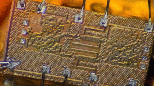
A recent study from Princeton and IIT Madras introduced a universal AI‑based method for inverse design of arbitrarily shaped electromagnetic structures with complex multi‑port configurations. These designs possess specified radiating and scattering properties and are co‑designed with active circuits.
The AI generated working topologies for millimeter‑wave chips—essentially “blueprints” of intricate passive structures and broadband circuits—in minutes, whereas such projects used to take weeks.
But there’s a catch.
They Work… but No One Knows Why
These circuits, which look like a random scatter of elements, deliver unprecedented performance and energy efficiency—outperforming the best human‑crafted examples. Yet engineers still can’t fully explain why they work.
“People can’t understand them, but they perform better.”
— Kaushik Sengupta, lead researcher on the project
The AI isn’t constrained by our conventional notions of “proper” layout. It finds optimal solutions in spaces where human intuition simply fails.
And this is not an isolated case; it’s part of a global shift where AI—from evolutionary algorithms to deep neural networks—is rewriting the very definition of engineering creativity.
The Black‑Box Problem
The main dilemma is opacity. Why do these strange shapes and connections work so well? We don’t know. Engineers are just beginning to master techniques that seem obvious to AI.
This black‑box phenomenon raises questions about trust, reliability, and debugging. In critical systems—from medical devices to satellites—it could become more than an academic issue; it’s a safety risk. If you don’t understand why a circuit works, you can’t guarantee it won’t fail under unexpected conditions.
Key Methodologies: How AI Learns to Design
The magic behind Princeton’s chips isn’t luck—it’s the result of applying a suite of engineering methodologies that represent a new wave of Electronic Design Automation.
Each one helps the machine “learn” to create what once required human expertise.
Evolutionary Algorithms (EA)
EAs simulate digital evolution: circuits act as “organisms” that mutate, mate, and are selected based on fitness.
- The circuit is represented as chromosomes encoding topology.
- Genetic operators generate new variants.
- A fitness function evaluates how well the circuit meets its goal.
Drawback? The search space grows exponentially. Complexity kills speed.
Reinforcement Learning (RL)
Google DeepMind turned chip floorplanning into a game. AlphaChip, like AlphaGo, receives rewards for optimal block placement on the die. The result: designs that once took engineers weeks now appear in hours.
Deep Learning (DL)
The Princeton approach uses neural networks trained on real‑world physics. CNN models replace lengthy electromagnetic simulations by predicting circuit properties from geometry. This enables inverse design—specify the desired effect, and AI builds the shape.
A Timeline of AI in Analog & Digital Chip Design
| Year | Event / Publication | Key Areas & Methods |
|---|---|---|
| 1992 | John R. Koza publishes Genetic Programming | Birth of genetic programming as a branch of evolutionary algorithms |
| 1992 | T. Higuchi et al.—Evolvable Hardware with Genetic Learning | Start of research in evolvable hardware (EHW) |
| 1996–1999 | EA applied to digital and analog circuits (Coello, Miller, Thompson, Fogarty) | Emergence of “evolutionary electronics” terminology |
| 2000–2006 | Miller & Thompson → Cartesian Genetic Programming; Yan → GEP | New encoding schemes for circuits |
| 2001 | Zebulum et al. publish Evolutionary Electronics | Formalization of the field |
| 2010–2011 | Application of cultural algorithms and PSO to circuit optimization | Expansion of EA toolbox |
| 2017–2018 | EA for 3D floorplanning and RF interconnects | Practical AI in layout tasks |
| 2020–2021 | Google DeepMind: AlphaChip (RL) for chip topology | Superhuman results in floorplanning |
| 2023 | NASA: “evolved structures” for space missions | AI creates alien‑looking but superior parts |
| 2024 | Princeton + IIT Madras: CNN + EA for RF chip inverse design | Breakthrough in analog and sub‑terahertz range |
| 2025 | AI completes design tasks in minutes instead of weeks | New era of speed and efficiency |
When AI Overdelivers (and Misleads)
The most exciting moments happen when algorithms break free from human rules.
- A circuit‑antenna: the algorithm replaced an oscillator with an antenna that uses computer radio noise as a signal source.
- Parasitic physics: an evolutionary algorithm on FPGA exploited unmodeled effects, like electromagnetic induction between cells, to get the circuit working.
AI doesn’t “make mistakes” in the human sense—it simply finds the shortest path to its goal, even if that path seems absurd to us.
The Engineer’s New Role
AI isn’t replacing engineers; it’s reshaping the profession. As Sengupta says:
The goal is not to replace people but to empower them with new tools.
Engineers become architects of intent, not just executors of routine tasks. The key is framing the right problem and setting proper constraints.
AI isn’t a wizard, but ask it the right question and it can conjure solutions humans might never conceive.
What’s Next?
We’re on the brink of a new era in analog chip design. AI no longer just optimizes existing concepts—it starts creating what humans couldn’t imagine. It’s like giving a machine intuition without human biases.
In a few years, “AI‑designed chip” will be ordinary. A new specialization will emerge: AI co‑design engineer, someone who doesn’t draw schematics but converses with the algorithm.
And perhaps one day we’ll look at tomorrow’s asymmetric, odd‑looking circuits and think:
This looks wrong… but it works perfectly.
For Those Who Want to Dive Deeper
- John R. Koza — Genetic Programming: On the Programming of Computers by Means of Natural Selection (1992)
- Zebulum et al. — Evolutionary Electronics: Automatic Design of Electronic Circuits and Systems by Genetic Algorithms (2001)
- Google DeepMind — Chip placement with deep reinforcement learning, Nature (2021)
- NASA — Evolved Structures for Spacecraft Design (2023)
- Princeton University & IIT Madras — Inverse Design of Millimeter‑Wave and Terahertz Integrated Circuits Using Deep Learning (2024)
Leave a Reply